THE UniBO FINGERPRINT CAPACITIVE SENSOR
SGS-Thomson
Innovative System Design group at University
of Bologna, ITALY
Designer: M.
Tartagni
System & Interface Engineering:
M. Bisio and R. Rambaldi
Pattern Recognition:
Zs. V. Kovacs
Head: Prof.
R. Guerrieri
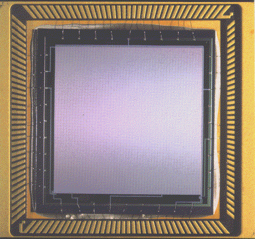
On September 1996 we demonstrated the first working prototype of
a microchip that can directly register the pattern of a human fingertip,
detecting variations in the electrical field existing between ridges and
valleys of the skin and sensor surface. Compared to other sensing approaches
currently available, this technology offers superior greyscale image quality
and a direct route to the digital information used in the personal identification
process. We were able to overcome the difficult problem of sensing ultra-small
capacitances thanks to the feedback capacitive sensing
scheme (FCS) that we introduced.
 In
a technical
paper presented at the 1997 International
Solid State Circuit Conference in San Francisco has been reported a
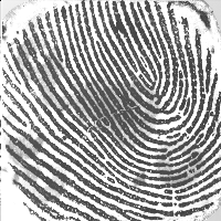
sensor array that 'grabs' a fingerprint pattern without using an optical
or mechanical adaptor such as a scanner or camera. When the finger is placed
onto the chip's silicon surface, the capacitive sensors register the fingerprint
pattern by interacting with electric field variations produced by the skin's
ridges and valleys. The chip then creates an electrical representation
of a fingerprint. This offers a new dimension in the arena of biometrics.
Some of the security applications for this electronic fingerprint imaging
sensor include PC access, electronic security for internet transactions,
physical identification for access to automobiles and buildings, Person
Identification Number (PIN) replacement, as well as applications in the
smartcard, appliance and portable electronics fields. A full paper
regarding this sensor appeared on the January 1998 issue of the IEEE Journal
of Solid State Circuits.
In
a technical
paper presented at the 1997 International
Solid State Circuit Conference in San Francisco has been reported a
sensor array that 'grabs' a fingerprint pattern without using an optical
or mechanical adaptor such as a scanner or camera. When the finger is placed
onto the chip's silicon surface, the capacitive sensors register the fingerprint
pattern by interacting with electric field variations produced by the skin's
ridges and valleys. The chip then creates an electrical representation
of a fingerprint. This offers a new dimension in the arena of biometrics.
Some of the security applications for this electronic fingerprint imaging
sensor include PC access, electronic security for internet transactions,
physical identification for access to automobiles and buildings, Person
Identification Number (PIN) replacement, as well as applications in the
smartcard, appliance and portable electronics fields. A full paper
regarding this sensor appeared on the January 1998 issue of the IEEE Journal
of Solid State Circuits.
Compared to alternate personal identification methods such as infrared
and retinal scans, the electronic fingerprint technology provides heightened
security, ease-of-use and cost benefits. This compact one-chip solution
is smaller in size and ultra-low power compared to optical methods, consuming
less than 1mW at 5V. It also generates higher image quality than most other
identification methods, including technologies based on heat. Since the
chip's pixels are on a pitch of more than 25µm, it can be easily
integrated into standard CMOS technology, the digital microprocessing common
to desk top computers, to keep costs low.
Description of the design
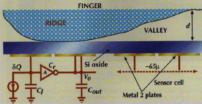 The
live fingerprint imager is based on a feedback capacitive sensing scheme.
Two metal-2 plates are placed adjacently in the cell area and separated
from the skin surface by the passivation oxide. The skin surface can be
thought of as a third plate opposed to the metal-2 ones and separated by
a dielectric layer with variable thickness composed of air.
The
live fingerprint imager is based on a feedback capacitive sensing scheme.
Two metal-2 plates are placed adjacently in the cell area and separated
from the skin surface by the passivation oxide. The skin surface can be
thought of as a third plate opposed to the metal-2 ones and separated by
a dielectric layer with variable thickness composed of air.
From a lumped-model point of view, this structure realizes a two series-connected
capacitors scheme. The metal-2 plates are separately connected to the input
and out of a high-gain inverter, thus realizing a charge integrator.
The cell works in two phases: first, the charge amplifier is reset,
shorting input and output of the inverter. During this phase, output of
the inverter settles to its logical threshold. During the second phase,
a fixed amount of charge is sinked from the input, causing an output voltage
swing inversely proportional to feedback capacitance value. Since feedback
capacitance in inversely proportional to the distance of the skin, a linear
dependence of output voltage on skin distance is expected. For a fixed
amount of sinked charge, the output voltage of the inverter will range
between two extremes depending on feedback capacitance value: 1) the upper
saturation level if no feedback capacitance is present; 2) a value close
to the logical threshold when the feedback capacitance is large.
The current prototype is able to capture a fingerprint image at 390
dpi, enough to provide high-reliability fingerprint matching based on image
processing algorithms. Future prototypes are expected to increase resolution
to as much as 512 dpi.
Since the distance between the skin and sensor identifies the presence
of ridges and valleys, an array of cells is used to sample the fingerprint
pattern. An array of cells is addressed in a raster mode by means of horizontal
and vertical scanners. The chip also contains timing control and voltage
references.
Since the pixels are on a pitch of more than 25µm, the architecture
is integrated in standard CMOS technology by SGS-Thomson. The power consumption
at 10 frame/s is below 1mW for continous acquisition.
Fingerprint
database
FAQs will be soon available
FOR TECHNICAL QUESTIONS
|
MARCO TARTAGNI c/o DEIS Universita' di Bologna, Viale Risorgimento
2, I-40136 Bologna, ITALY, tel: +39-(51)-644-3557, fax: +39-(51)-644-3073
e-mail: mtartagni@deis.unibo.it
|
FOR BUSINESS QUESTIONS
|
ALAN KRAMER c/o SGS-Thomson Innovative Systems Design Group,
2115 Milvia st. Suite 301 Berkeley, CA, 94704-1112, USA; tel: +1-510-647-1200,
fax: +1-510-665-9730
e-mail: alan.kramer@st.com
|
© 1998 IEEE. Personal use of this material
is permitted. However, permission to reprint/republish this material for
advertising or promotional purposes or for creating new collective works
for resale or redistribution to servers or lists, or to reuse any copyrighted
component of this work in other works must be obtained from the IEEE.
© 1997 SGS-Thomson Microelectronics