updated 2000.03.30
Author Janez Puhan
D Flip-flop As A Frequency Divider
The circuit
The D flip-flop, as shown below, is constructed by replacing the gates in the latch flip-flop with cross-coupled NAND gates.
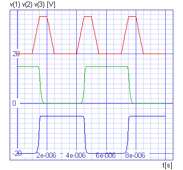
D stands for "Delay" and refers to the fact that the binary value at D will be shifted to the output Q by positive clock pulse edge at the input T. When the signal at D is changing, it will be shifted to Q at a subsequent positive clock edge only. Connecting the input D to the inverting output results in a frequency divider commonly known as count-by-two circuit.

The input file
d flip-flop as a frequency divider

.control
tran 0.1us 10us
plot v(1)+20 v(2) v(3)-20 xlabel t[s] ylabel 'v(1) v(2) v(3) [V]'
  + title 'TRAN analysis'
.endc

v1 1 0 dc 0 pulse 0 15V 1us 0.5us 0.5us 0.5us 3us

x1 8 7 6 nand2mos
x2 1 6 8 nand2mos
x3 8 1 7 4 nand3mos
x4 2 4 7 nand2mos
x5 2 8 3 nand2mos
x6 4 3 2 nand2mos

.subckt nand2mos 1 2 3
v1 4 0 dc 15V

c1 1 0 5pF
c2 2 0 5pF

m1 3 1 4 4 noname1
m2 3 2 4 4 noname1
m3 5 1 0 0 noname2
m4 3 2 5 5 noname2

.model noname1 pmos
.model noname2 nmos
.ends

.subckt nand3mos 1 2 3 4
v1 5 0 dc 0 pulse 0 15V

c1 1 0 5pF
c2 2 0 5pF
c3 3 0 5pF

m1 4 3 5 5 noname1
m2 4 2 5 5 noname1
m3 4 1 5 5 noname1
m4 4 3 7 7 noname2
m5 7 2 6 6 noname2
m6 6 1 0 0 noname2

.model noname1 pmos
.model noname2 nmos
.ends

.end
The results