
updated 2000.12.08
Author Janez Puhan
NAND And NOR Gates
Digital simulation can be accomplished using different levels of sophistication. The lowest level is the so called switch level which uses polynomial sources, followed by an inverter which uses a pair of complementary transistors as shown in the preceding case. Next is the Boolean gate level with NAND and NOR gates made from complementary MOS transistors. And finally, the functional model level of flip-flops, shift registers or decoders, can be built up with the gate level elements. In following case, circuits are simulated at the gate level.
In the past, TTL gates were popular with designers. Today, CMOS gates have virtually taken over as the device of choice. A few of reasons for this choice are excellent noise immunity, fast propagation delay times, and very low quiescent power operation. Moreover, they operate from a single power supply over a wide voltage range. Input capacitances are in the range of a few picofarads, thus keeping power dissipation at moderate levels even at high clock rates.
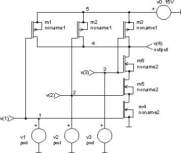
The circuit 1
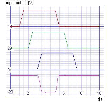
The input file 1
nand gate

.control
tran 0.5s 10s
plot v(1)+40 v(2)+20 v(3) v(4)-20 xlabel t[s] ylabel 'input output [V]'
  + title 'TRAN analysis'
.endc

vO 5 0 dc 15V
v1 1 0 dc 0 pwl 0 0 1s 0 1.5s 15V 5s 15V 5.5s 0 10s 0
v2 2 0 dc 0 pwl 0 0 2s 0 2.5s 15V 6s 15V 6.5s 0 10s 0
v3 3 0 dc 0 pwl 0 0 3s 0 3.5s 15V 7s 15V 7.5s 0 10s 0

m1 4 1 5 5 noname1
m2 4 2 5 5 noname1
m3 4 3 5 5 noname1
m4 6 1 0 0 noname2
m5 7 3 6 6 noname2
m6 4 2 7 7 noname2

.model noname1 pmos
.model noname2 nmos

.end
The results 1
The circuit 2

The input file 2
nor gate

.control
tran 0.5s 10s
plot v(1)+40 v(2)+20 v(3) v(4)-20 xlabel t[s] ylabel 'input output [V]'
  + title 'TRAN analysis'
.endc

v0 5 0 dc 15V
v1 1 0 dc 0 pwl 0 0 1s 0 1.5s 15V 5s 15V 5.5s 0 10s 0
v2 2 0 dc 0 pwl 0 0 2s 0 2.5s 15V 6s 15V 6.5s 0 10s 0
v3 3 0 dc 0 pwl 0 0 3s 0 3.5s 15V 7s 15V 7.5s 0 10s 0

m1 4 1 0 0 noname2
m2 4 2 0 0 noname2
m3 4 3 0 0 noname2
m4 6 1 5 5 noname1
m5 7 2 6 6 noname1
m6 4 3 7 7 noname1

.model noname1 pmos
.model noname2 nmos

.end
The results 2
