
updated 2000.12.08
Author Janez Puhan
Inverters With Comlementary Semiconductors
The circuit 1
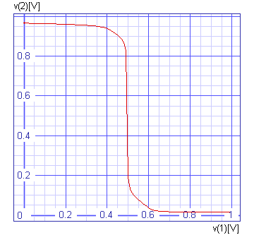
In this case, two inverters are sketched out. The first example depicts two complementary bipolar transistors supplied with a dc voltage of 1V. Binary transition from Low = 0 to High = 1 takes place when half of the supply voltage is placed on the input. In contrast to the polynomials gates, where the transition is linear, a realistic S-like characteristic is present. Binary variables at the output, therefore, are clamped to ground or the supply voltage. In order to avoid the error message "timestep to small", the switching times of transistors have to be adjusted from their default values to a realistic value using the base resistor rb and collector capacitance cjc.
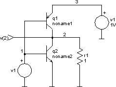
The input file 1
inverter with complementary bipolar transistors

.control
dc v1 0 1V 0.01V
plot v(2) xlabel v(1)[V] ylabel v(2)[V] title 'DC analysis'
.endc

v0 3 0 dc 1V
v1 1 0 dc 0

R1 2 0 1

q1 2 1 3 noname1
q2 2 1 0 noname2

.model noname1 pnp is=0.1u rb=1 cjc=1n
.model noname2 npn is=0.1u rb=1 cjc=1n

.end
The results 1
The circuit 2
The above circuit has never gained significant acceptance. Technological difficulties were unsolvable when trying to integrate a bipolar pair on a single monolithic chip. On the contrary, integration of complementary symmetric field effect transistors has been done successfully. In the next example, the CMOS logic inverters, 4007/4049, are shown. The approximate sizes of the crystal structures are specified in the netlist below. Note, that when using semiconductors, it is customary to provide some amount of realistic junction capacitance. If the correct value is not known, then using between 3 and 10pF is acceptable. Realistic models are the key to successfully avoiding dc and transient convergence problems.

The input file 2
inverter with complementary FETs

.control
tran 0.5n 50n
plot v(2)+5 v(3)-10 xlabel t[s] ylabel 'v(2) v(3) [V]' title 'TRAN analysis'
.endc

v0 4 0 dc 10V
v1 1 0 dc 0 pulse 0 10V 5ns 0 0 10ns 1s

r1 1 2 50
r2 3 0 1k

c1 2 3 3pF

d1 2 4 diode
d2 0 2 diode

m1 3 2 4 4 pkanal w=250u l=6u
m2 3 2 0 0 nkanal w=250u l=3u

.model diode d (cjo=3.5pF mj=0)
.model pkanal pmos
.model nkanal nmos

.end
The results 2
