updated 2000.12.08
Author Janez Puhan
Polynomial Representation Of Logic Gates
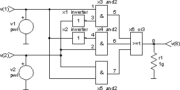
The circuit
The boolean functionality of logic gates may be approximated with simple polynomial sources. A logic inverter for example may be simulated with a polynomial voltage source (first order):
voltage = p0 + p1 * xa + p2 * xa^2 + ...
inverter = 1 - xa (with p0 = 1 and p1 = -1)
Gates with two inputs can be simulated with a polynomial source of 2 dimensions (second order):
voltage = p0 + p1 * xa + p2 * xb + p3 * xa^2 + p4 * xa * xb + p5 * xb^2 + ...
| and2 = xa * xb | (p0 = 0, p1 = 0, p2 = 0, p3 = 0, p4 = 1) |
| or2 = xa + xb - xa * xb | (p0 = 0, p1 = 1, p2 = 1, p3 = 0, p4 = -1) |
| nand2 = 1 - xa * xb | (p0 = 1, p1 = 0, p2 = 0, p3 = 0, p4 = -1) |
| nor2 = 1 - xa - xb + xa * xb | (p0 = 1, p1 = -1, p2 = -1, p3 = 0, p4 = 1) |
| exor2 = xa + xb - 2 * xa * xb | (p0 = 0, p1 = 1, p2 = 1, p3 = 0, p4 = -2) |
| exnor2 = 1 - xa - xb + 2 * xa * xb | (p0 = 1, p1 = -1, p2 = -1, p3 = 0, p4 = 2) |
Accordingly, gates with three inputs can be represented by:
| p0 + p1 * xa + p2 * xb + p3 * xc + p4 * xa^2 + p5 * xa * xb + p6 * xa * xc + p7 * xb^2 + p8 * xb * xc + p9 * xc^2 + ... |
The input file
polynomial representation of logic gates
.control
tran 0.1s 10s
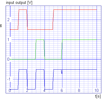
plot v(1)+1.5 v(2) v(8)-1.5 xlabel t[s] ylabel 'input output [V]'
+ title 'TRAN analysis'
.endc
v1 1 0 dc 0 pwl 0 0 0.9s 0 1s 1V 1.9s 1V 2s 0 4.9s 0 5s 1V 10s 1V
v2 2 0 dc 0 pwl 0 0 2.9s 0 3s 1V 3.9s 1V 4s 0 5.9s 0 6s 1V 10s 1V
r1 8 0 1g
x1 2 3 inverter
x2 1 4 inverter
x3 1 3 5 and2
x4 4 2 6 and2
x5 1 2 7 and2
x6 5 6 7 8 or3
.subckt inverter 1 2
r1 1 0 1g
r2 2 0 1g
b1 2 0 v = 1 - v(1)
.ends
.subckt and2 1 2 3
r1 1 0 1g
r2 2 0 1g
r3 3 0 1g
b1 3 0 v = v(1) * v(2)
.ends
.subckt or2 1 2 3
r1 1 0 1g
r2 2 0 1g
r3 3 0 1g
b1 3 0 v = v(1) + v(2) - v(1) * v(2)
.ends
.subckt or3 1 2 3 4
x1 1 2 5 or2
x2 3 5 4 or2
.ends
.end
The results