updated 2000.12.06
Author Janez Puhan
Audio Power Amplifier
The circuit
With preamplifiers, high gain and signal to noise ratio are the main objectives of the design. With power amplifiers, the highest possible undistorted power is the design objective. Within the total volume range, the output waveform always has to be a true image of input signal. This requirement is achieved mainly by negative feedback. However, there are limitations to this technique. The phase angle of the open loop gain increases with frequency, thus leading to possible instabilities by changing negative feedback into positive feedback. If b denotes the fraction of output voltage fed back to the input, and if A0 denotes the open loop gain, then the closed loop gain is determined by
The Nyquist stability criterion is a very useful means of determining the stability of an amplifier. If
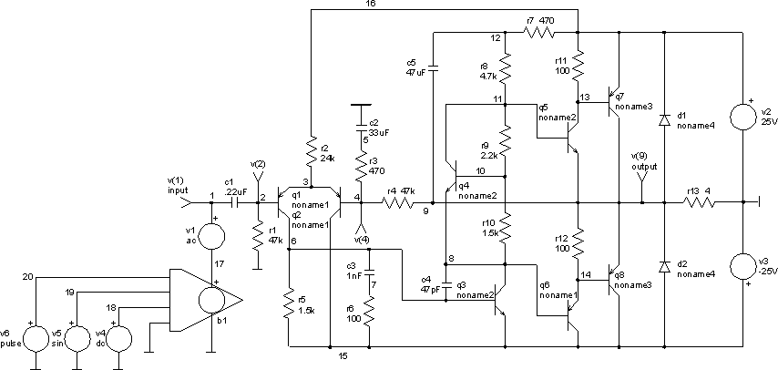
The input file
audio power amplifier
.control
tran 5us 1ms
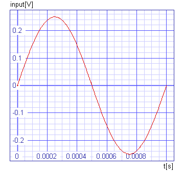
plot v(1) xlabel t[s] ylabel input[V] title 'TRAN sine response'
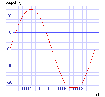
plot v(9) xlabel t[s] ylabel output[V] title 'TRAN sine response'
plot v(6,15) xlabel t[s] ylabel 'diferential output[V]' title 'TRAN sine response'
plot v(2,4) xlabel t[s] ylabel 'diferential_input[V]' title 'TRAN sine response'
* switch to ac input
alter v4 dc = 0
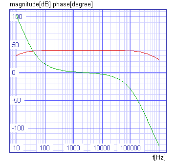
ac dec 25 10Hz 1megHz
set units = degress
plot vdb(9) vp(9) xlabel f[Hz] ylabel 'magnitude[dB] phase[degree]'
+ title 'AC analysis'
* switch to pulse input
alter v4 dc = -1
tran 25ns 15us
plot v(1)+0.3 v(9)/100 v(2,4)-0.3 xlabel t[s]
+ ylabel 'input / output / diferential input [V]' title 'TRAN pulse response'
.endc
v1 1 17 dc 0 ac 1
v2 16 0 dc 25V
v3 15 0 dc -25V
v4 18 0 dc 1V
v5 19 0 dc 0 sin 0 0.25V 1kHz
v6 20 0 dc 0 pulse 0 0.2V 0.5us 0 0 7.5us 1s
c1 1 2 0.22uF
c2 5 0 33u
c3 7 6 1n
c4 6 8 47p
c5 9 12 47u
r1 2 0 47k
r2 3 16 24k
r3 4 5 470
r4 4 9 47k
r5 6 15 1.5k
r6 15 7 100
r7 12 16 470
r8 12 11 4.7k
r9 11 10 2.2k
r10 10 8 1.5k
r11 16 13 100
r12 9 14 100
r13 9 0 4
b1 17 0 v = v(18) * ((v(18) + 1) * v(19) + (v(18) - 1) * v(20)) / 2
q1 6 2 3 noname1
q2 15 4 3 noname1
q3 8 6 15 noname2
q4 11 10 8 noname2
q5 13 11 9 noname2 area=10
q6 15 8 14 noname1 area=10
q7 9 13 16 noname3
q8 15 14 9 noname3
d1 9 16 noname4
d2 15 9 noname4
.model noname1 pnp (is=1.1p bf=200 nf=1.21 vaf=50 ikf=.1
+ ise=13p ne=1.9 br=6 rc=.6 rb=40 cje=23p vje=.85 mje=1.25
+ tf=.5n cjc=19p vjc=.5 mjc=.2 tr=34n xtb=1.5 kf=.3f af=1)
.model noname2 npn (is=1.1p bf=200 nf=1.21 vaf=50 ikf=.1
+ ise=13p ne=1.9 br=6 rc=.6 rb=40 cje=23p vje=.85 mje=1.25
+ tf=.5n cjc=19p vjc=.5 mjc=.2 tr=34n xtb=1.5 kf=.3f af=1)
.model noname3 pnp (is=15n bf=75 nf=1.67 vaf=100 ikf=4
+ br=4 rc=.06 cje=520p vje=1.2 mje=.5 tf=40n cjc=380p
+ mjc=.45 tr=.8u xtb=1.5)
.model noname4 d (rs=0.04 is=1.4n n=1.7 vj=0.34 mj=0.38)
.end
The results