updated 2000.03.30
Author Janez Puhan
Regulated DC Power Supply
The circuit
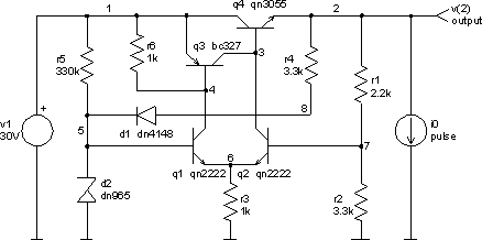
A conventional dc series regulator is shown below. The output voltage at node 2 needs to be regulated. Transistors q1 and q2form a differential amplifier which compares the commanded voltage at node 5 with the real voltage at node 7. Possible differences are sensed and amplified, and control a power transistor, q4, operating in a continuous conduction mode. Any variation of the input voltage or load current causes the series transistor to become more or less conducting, thus effectively stabilising the output voltage.
The input file
regulated dc voltage supply
.control
dc v1 25V 30V 0.1V
alter i0 dc = 5A
dc v1 25V 30V 0.1V
alter i0 dc = 10A
dc v1 25V 30V 0.1V
plot dc1.v(2) dc2.v(2) dc3.v(2) xlabel v1[V] ylabel output[volt] title 'DC analyses'
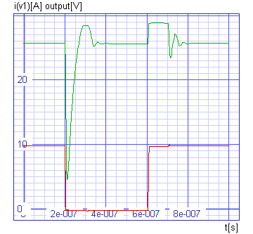
tran 5ns 1us
plot (i(v1)+10)*10+10 v(2) xlabel t[s] ylabel 'i(v1)[A] output[V]'
+ title 'TRAN analysis'
.endc
v1 1 0 dc 30V
i0 2 0 dc 0 pulse 10A 11A 0.2us 0 0 0.4us 1s
r1 2 7 2.2k
r2 7 0 3.3k
r3 6 0 1k
r4 8 2 3.3k
r5 5 1 330k
r6 1 4 1k
d1 8 5 dn4148
d2 0 5 dn965
q1 4 5 6 qn2222
q2 3 7 6 qn2222
q3 3 4 1 bc327
q4 1 3 2 qn3055
.model dn4148 d (rs=0.8 cjo=4pF is=7e-09 n=2 vj=0.6V tt=6e-09 mj=0.45 bv=100V)
.model dn965 d (rs=8.7297 bv=14.927 cjo=578.05p tt=20n n=2 is=1e-9
+ ibv=8.3333m)
.model qn2222 npn (is=1.9e-14 bf=150 vaf=100 ikf=.175 ise=5e-11 ne=2.5 br=7.5
+ var=6.38 ikr=.012 isc=1.9e-13 nc=1.2 rc=.4 xtb=1.5 cje=26pF tf=.5e-9
+ cjc=11pF tr=30e-9 kf=3.2e-16 af=1.0)
.model bc327 pnp (is=3.69e-14 nf=1 bf=133 vaf=120 ikf=1 ise=467f ne=2 br=4
+ nr=1 var=20 ikr=1.5 re=.563 rb=2.25 rc=.225 xtb=1.5 cje=104p cjc=46.8p
+ tf=722p tr=161n)
.model qn3055 npn (is=1.5e-8 nf=1.67 bf=75 vaf=100 ikf=4 br=4 rc=.06 mjc=.45
+ vje=1.2 mje=.5 xtb=1.5 cje=520pF tf=40e-9 cjc=380pF tr=.8u)
.end
The results