updated 2000.07.06
Author Janez Puhan
Controlled Flyback Converter
The circuit
A more efficient dc converter than the one in the previous example is shown next. It is based on the flyback principle. When MOSFET, x7, is turned on, the drain current rises linearly with time, therefore, the magnetic energy, i(v0)peak2 * l2 / 2, is stored in the core of the transformer. When x7 is turned off, the polarity of the voltages at inductances l2, l3 and l4 change, and the stored energy is transferred to the output via d3 and d4. dc power taken from the battery, v0, is proportional to the frequency of operation, thus P = l2 * f * i(v0)peak2 / 2. Because of the losses in the semiconductors and the transformer, about 80% of the energy is available at the output terminals.
Stabilisation of dc output voltages is accomplished by pulsewidth control. When the voltage level is too high, the transistor in the opto-coupler, x8, starts to conduct. Capacitor, c3, acting as a differentiator, will be discharged faster, thus reducing the turn on time and lengthening the turn off time of the power MOSFET while the period of operation remains constant. When the output voltage is too low, the turn on time will increase, correspondingly. The timing oscillator, differentiator, and pulse forming circuit are realised with 4049 CMOS buffers. For simplicity, a subcircuit,

The input file
controlled flyback converter
.control
tran 0.5us 100us uic
plot v(2)+15 v(3) v(5)-10 v(7)-25 xlimit 10u 100u xlabel t[s]
+ ylabel 'v(2) v(3) v(5) v(7)[V]' title 'TRAN analysis'
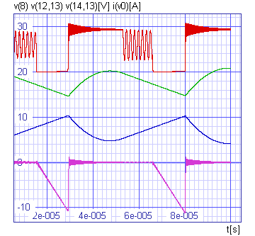
plot v(8)/4+20 (v(12,13)-20)*20+20 (v(14,13)+20)*20+5 i(v0)*4
+ xlimit 10u 100u xlabel t[s] ylabel 'v(8) v(12,13) v(14,13)[V] i(v0)[A]'
+ title 'TRAN analysis'
.endc
v0 9 0 dc 24V
r1 19 14 750
r2 4 0 3.9k
r3 4 5 100
r4 15 7 100
r5 16 17 4.7k
r6 12 13 100
r7 14 13 100
r8 0 13 100meg
r9 19 0 100meg
l1 1 2 4.7mH
l2 8 9 120uH
l3 10 13 275uH
l4 13 11 275uH
k23 l2 l3 0.9975
k24 l2 l4 0.9975
k34 l3 l4 0.9975
c1 1 0 27nF
c2 2 0 33nF ic=10V
c3 3 4 10nF ic=1V
c4 5 15 1nF
c5 17 16 0.1uF ic=30V
c6 16 0 22uF ic=10V
c7 12 13 22uF ic=20V
c8 13 14 22uF ic=20V
d1 0 16 zener1
d2 18 12 zener2
d3 10 12 dn5811
d4 14 11 dn5811
d5 8 17 dn5811
x1 1 2 16 cmos
x2 2 3 16 cmos
x4 6 7 16 cmos
x5 6 7 16 cmos
x6 6 7 16 cmos
x3 5 6 16 cmos
x7 8 7 0 mospwr
x10 18 19 4 0 optokop
.model zener1 d (rs=10 bv=10)
.model zener2 d (rs=50 bv=36)
.model dn5811 d (is=0.4u rs=0.007 n=1.8 tt=22n cjo=135p vj=0.6 mj=0.38 bv=190
+ ibv=3mA)
.subckt cmos 1 2 3
m1 2 1 3 3 p4049 w=250u l=6u
m2 2 1 0 0 n4049 w=250u l=3u
d1 1 3 diode
d2 0 1 diode
.model diode d (cjo=3.5p mj=0)
.model n4049 nmos level=3
.model p4049 pmos level=3
.ends
.subckt mospwr 10 20 30
rg 20 2 15
rd 10 1 0.141
rds 1 3 1.78meg
rcg 4 1 10meg
cgd 4 1 787pF
ls 30 3 10nH
ecg 5 2 2 1 1
edg 7 1 1 2 1
dgd 2 6 dcgd
dds 3 1 dsub
m1 1 2 3 3 dmos l=1u w=1u
mcg 4 5 2 2 sw l=1u w=1u
mdg 6 7 1 1 sw l=1u w=1u
.model dcgd d (cjo=787p mj=0.5 vj=0.41)
.model dsub d (is=144f rs=0 vj=0.8 mj=0.4 cjo=1.2n tt=576n)
.model dmos nmos (level=3 vmax=17.1meg theta=63.6m vto=3.3 kp=9 rs=8.5m
+ is=144f cgso=1.9m)
.model sw nmos (level=3 vto=0 kp=0.45)
.ends
.subckt optokop 1 2 3 4
vm 6 2 dc 0
f1 3 5 vm 0.005
d1 1 6 diode
q1 3 5 4 trans
.model diode d (n=2 rs=0.7 cjo=40p)
.model trans npn (is=25p ikf=0.1 vaf=100 tr=0.15u br=10 cjc=25p)
.ends
.end
The results