
updated 2000.03.30
Author Janez Puhan
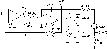
Multiple Waveform Generator
The circuit
The circuit generates a triangle and sine signal. It comprises a comparator, an integrator and a JFET. The opamp x1 (comparator) compares the square and triangle signal. Whenever the node 1 voltage reaches zero, x1 switches its output. This causes the integration capacitor to be charged in the opposite direction until the comparator senses zero voltage again. The oscillation frequency depends on the time constant of the integrator (r2 and c1) and its hytheresis (r1 and r3). The triangle signal is converted to sine using a JFET. The harmonic distortion is minimal (1%) when the amplitude of v(4) is 3.5V.
The input file (multiple_waveform_generator.cir)
multiple waveform generator

* frequency fo = 1 / (4 r2 r3 c1 / r1)

.control
tran 2us 170ms 120ms
plot v(2) 4*v(4) 10*v(7) xlabel t[s] ylabel 'v(2) v(4) v(7) [V]'
  + title 'TRAN analysis'
.endc

x1 0 1 2 opamp
x2 3 0 4 opamp

r1 2 1 43k
r2 2 3 10k
r3 4 1 10k
r4 4 5 1meg
r5 5 0 1meg
r6 4 6 100
r7 7 0 100

c1 3 4 1uF

d1 4 5 dn4148
d2 0 5 dn4148

j1 7 5 6 jn3820

.subckt opamp 1 2 3
v1 5 0 dc 15V
v2 6 0 dc -15V

c0 2 0 1nF

e1 4 0 2 1 -100k

m1 3 4 5 5 pkanal w=100u l=10u
m2 3 4 6 6 nkanal w=100u l=10u

.model pkanal pmos
.model nkanal nmos
.ends

.model dn4148 d (rs=0.8 cjo=4pF is=7e-09 n=2 vj=0.6V tt=6e-09 mj=0.45 bv=100V)
.model jn3820 pjf (beta=1.27m lambda=40m vt0=-2.5V)

.end
The Results
