updated 2000.03.30
Author Janez Puhan
Sine Wave Oscillator With CMOS Inverter
The circuit
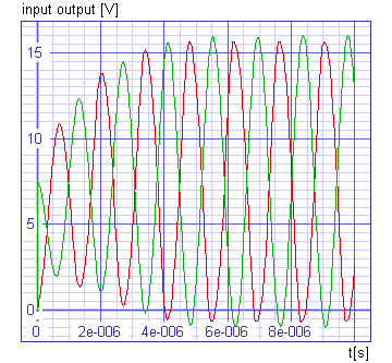
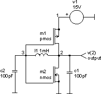
The circuit shown next presents an additional variant within the countless crowd of oscillator circuits. It can be used with digital systems as a time base generator because it can be easily realized with CMOS gates. The active element is an inverter which is built up of two complementary MOSFETs. Inductor, l1, connects the output to the input providing a negative dc feedback path. This causes the operating point to remain within the center of the transfer characteristic. Due to the high frequency of operation, the input and output capacitors, c1 and c2, are connected in series with their center tap attached to ground. Together, with l1, they form a high Q resonant circuit with nodes 2 and 3 in opposite phase. This satisfies the condition for oscillation.
The input file (sine_wave_oscillator_with_cmos_inverter.cir)
sine vawe oscillator with cmos inverter

* frequency of oscilation = 1 / (2 pi (l1 c1 c2 / (c1 + c2))^(1/2))

.control
tran 0.05us 10us uic
plot v(2) v(3) xlabel t[s] ylabel 'input output [V]' title 'TRAN analysis'
.endc

v1 1 0 dc 15V

l1 3 2 1mH

c1 2 0 100pF
c2 3 0 100pF ic=7.5V

m1 2 3 1 1 pmos
m2 2 3 0 0 nmos

.model pmos pmos
.model nmos nmos

.end
The results